Back in 2021 the IBM Telum processor, the heart of the IBM z16 mainframe, was unveiled at Hot Chips (video here). I watched the recording when it came out, absolutely glued to each little detail that was presented, even the ones I didn’t fully understand (after all, I’m not that much of a processor expert). Over the coming weeks, articles like this one from AnandTech would come out, diving deeper into the cache redesign: Did IBM Just Preview The Future of Caches? by Dr. Ian Cutress. Very cool stuff.
The truth is, every new mainframe has a new chip, and all of them have impressive new features that are innovative and exciting, but this is the first time in a long time that there was such a detailed technical splash with a named chip. What a roll out!
When I learned that Hot Chips would once again be hosted at Stanford, just across the bay from me, I jumped at the opportunity to attend for the next announcement: IBM Telum II
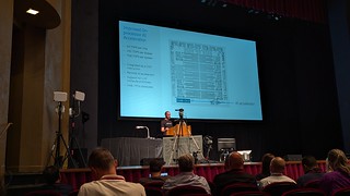
I was a little nervous about the event because of how deeply technical the sessions were on the hardware side, but I quickly found my stride. Since I haven’t kept up very closely on processor design, it was interesting to learn about Intel’s Lunar Lake processor, including the work they’ve done toward power reduction. But I’d say the general theme of the day was hardware accelerated AI on the processor. Telum II fit right in and Chris Berry gave a great presentation.
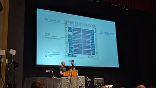
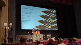
Now it’s time for me to geek out about it. As you can see, some of the big numbers that make this chip distinctive:
- A new built-in low-latency data processing unit (DPU) for accelerated IO
- 8 high-performance cores running at 5.5GHz
- 40% increase in on-chip cache capacity
- A new AI accelerator, the compute power of each accelerator is expected to be improved by 4x over Telum, reaching 24 trillion operations per second (TOPS)
See more on the full announcement from IBM and on the IBM Telum page.
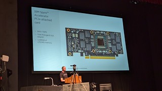
This time there was a second announcement too, the IBM Spyre Accelerator PCIe attached card. If you’re at all familiar with mainframes, you know that the PCIe drawers make up a nice chunk of the system, with cards to handle various functions that are separate from the compute drawer, which houses the processors and memory. Having a dedicated AI accelerator card was a logical step forward, so I was really excited to be there for its debut.
Again from the announcement linked above, “The Spyre Accelerator will contain 32 AI accelerator cores that will share a similar architecture to the AI accelerator integrated into the Telum II chip.”
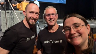
After the talk, I got to meet up with the other IBMers who were in attendance, which gave me the opportunity to meet Chris and Christian, who had spoken at the last Hot Chips.
At this event I also got to meet a couple folks from Chips and Cheese who were covering the event, and wrote an article that came out last week, Telum II at Hot Chips 2024: Mainframe with a Unique Caching Strategy, which was referenced in a recent Hackaday article Mainframe Chip Has 360MB Of On-Chip Cache and led to a few of my non-mainframe friends seeing it.
They also set up an interview with Susan Eickoff and Christian Jacobi, during which Susan shared view into development, beginning with how far out they have to plan (5+ years), a lead time that means its predecessor hasn’t even been released yet. I love these interviews because they give a public view into why certain things were designed in a specific way, which the community doesn’t often get to hear about from IBM. I wish we did more of these behind-the-scenes things at industry events that are so close to the tech community, there’s so much fascinating innovation happening at IBM and I still run into people who are surprised when they learn about it.
As I made my way around the event, I saw some more fascinating talks, but also got to meet a bunch of people. I spoke to a professor at Stanford and some of his students about open source and hardware architectures. I met Lori Servin of the RISC-V Foundation and got to geek out a bit over the talks I’ve been giving about porting open source software to various architectures.
I also got to spend a few minutes with Dr. Ian Cutress, who wrote the article on caches that I read three years ago (linked above).
In all, it was a great event and I’m grateful that I could attend. The following day I watched the live stream from home to check out what companies like Meta and Tesla are doing, plus a keynote from Victor Peng, President of AMD who spoke on our future of AI pervasiveness. It was a real stretch for me on a technical level, there are things I simply don’t understand and appreciate about chip design, but what I could follow (or quickly look up) made the event quite the learning experience.
